This project was based around moving homes constantly. Our aim was to produce collapsible furniture that could be easily adapted to everyday life and small spaces that students and the like would normally have to live in.


This project was based around moving homes constantly. Our aim was to produce collapsible furniture that could be easily adapted to everyday life and small spaces that students and the like would normally have to live in.

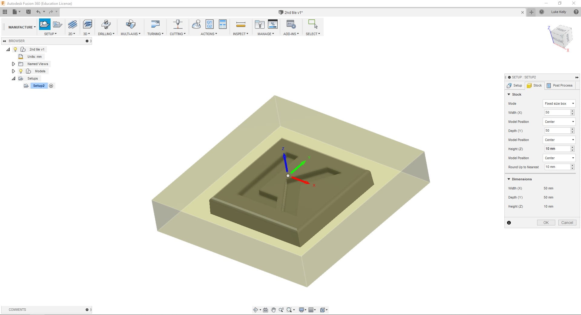
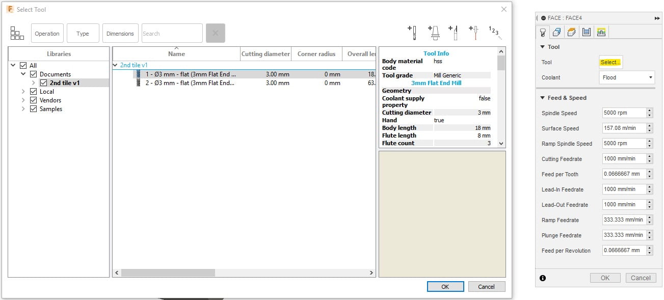
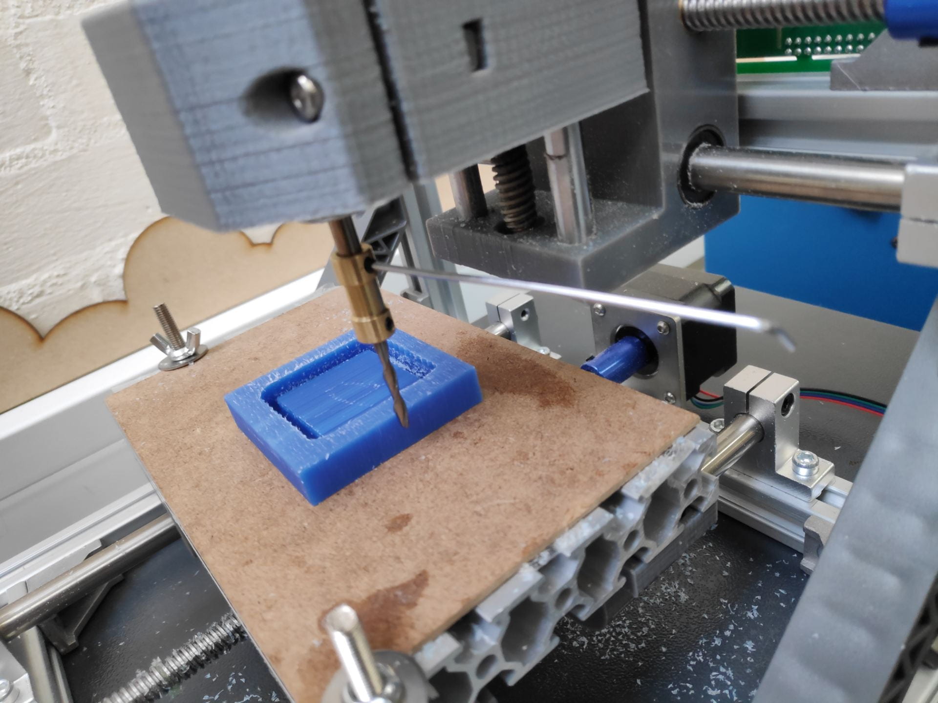
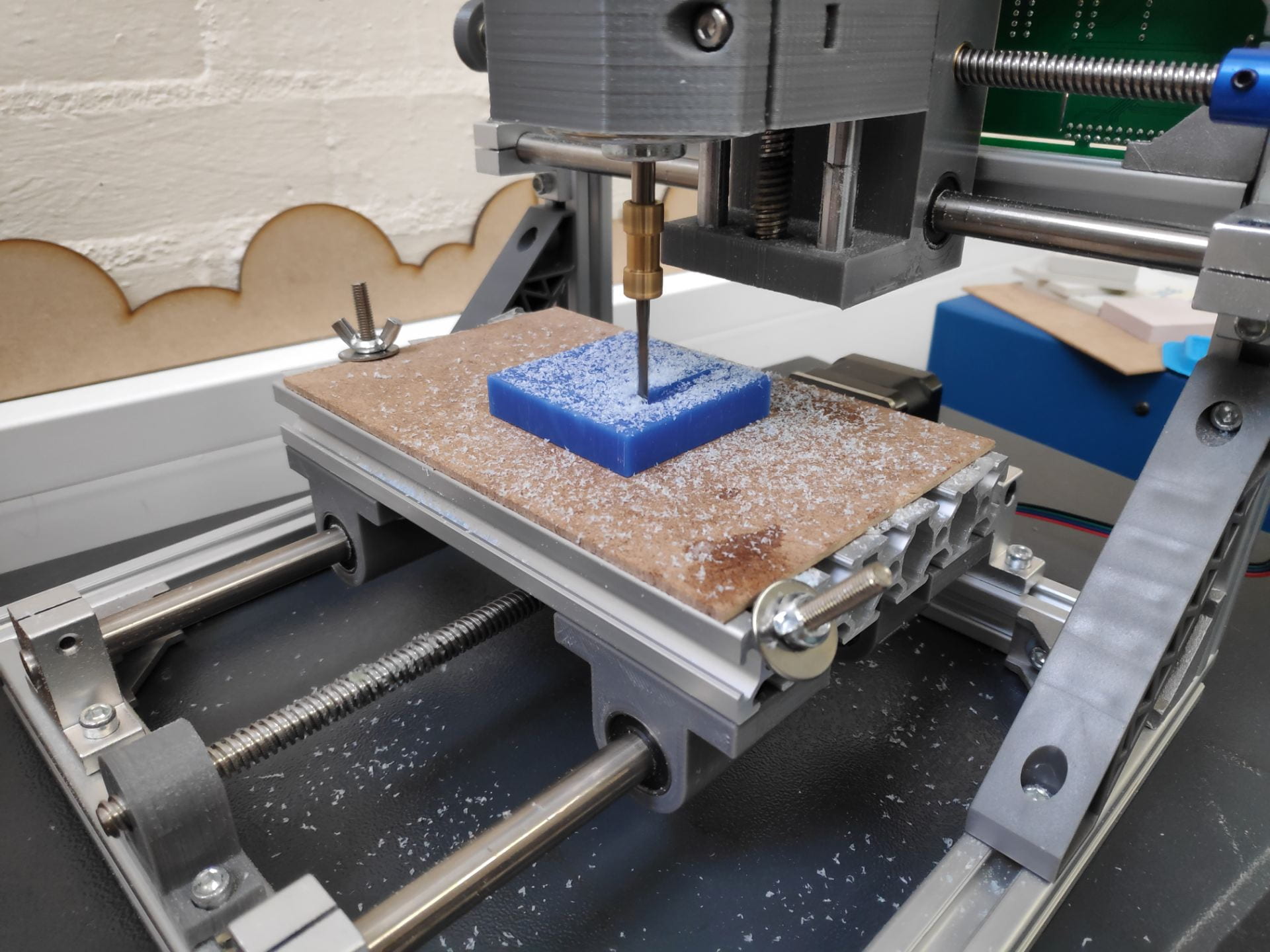
Most important is to know your cutter shape and size. Any features have to be designed in accordance to the diameter of the cutter as this will restrict how far and deep the slots between features can be.
Try and keep the cutter as big as possible as it will reduce cutting time as well as the chance of the cutter breaking or chipping.
If you are making a mould;just like the vacuum former; you will need to use draft angles even on small/short features.
Absolutely no undercuts as the CNC milling machine is unable to rotate the bed or spindle
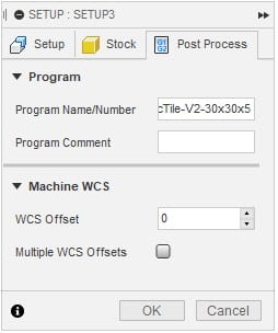


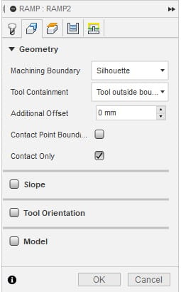
Relatively simple > Click Generate and choose Grbl as the post processor > check you save it in a place that you can find it and check the file name is correct and identifiable

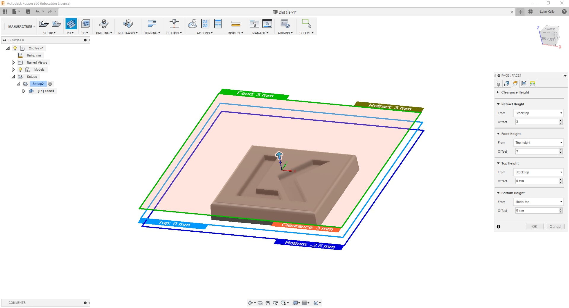
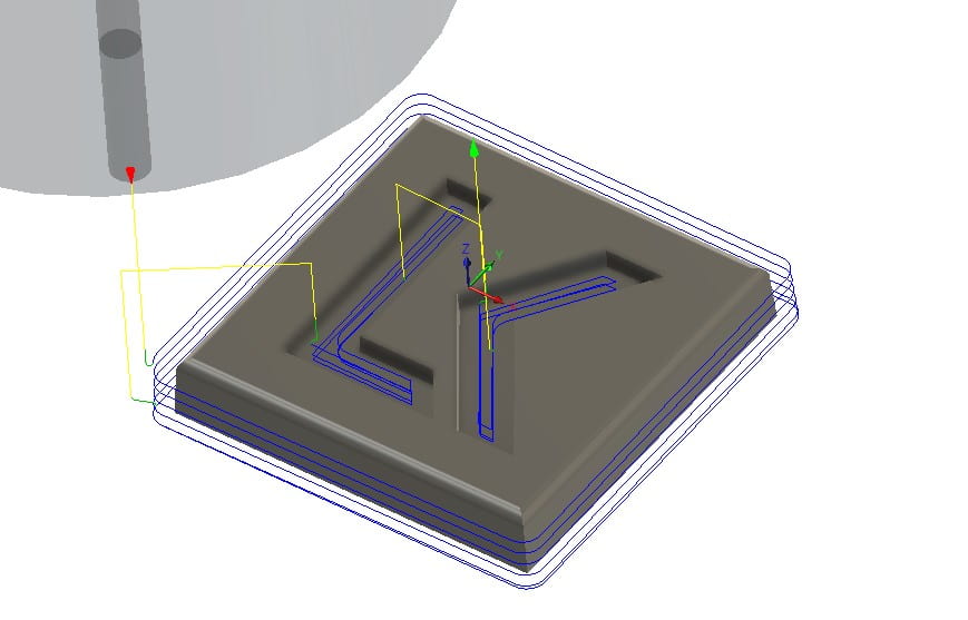
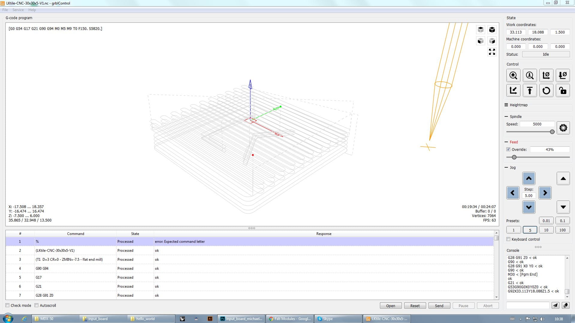
Here is the model with the tool path
Ensure that the milling cutter is tightened down before each use – it wasn’t checked in my case and it just popped off when it had nearly finished (no harm done!)
This meant that the operation had to be started again and therefore took much longer than it should have

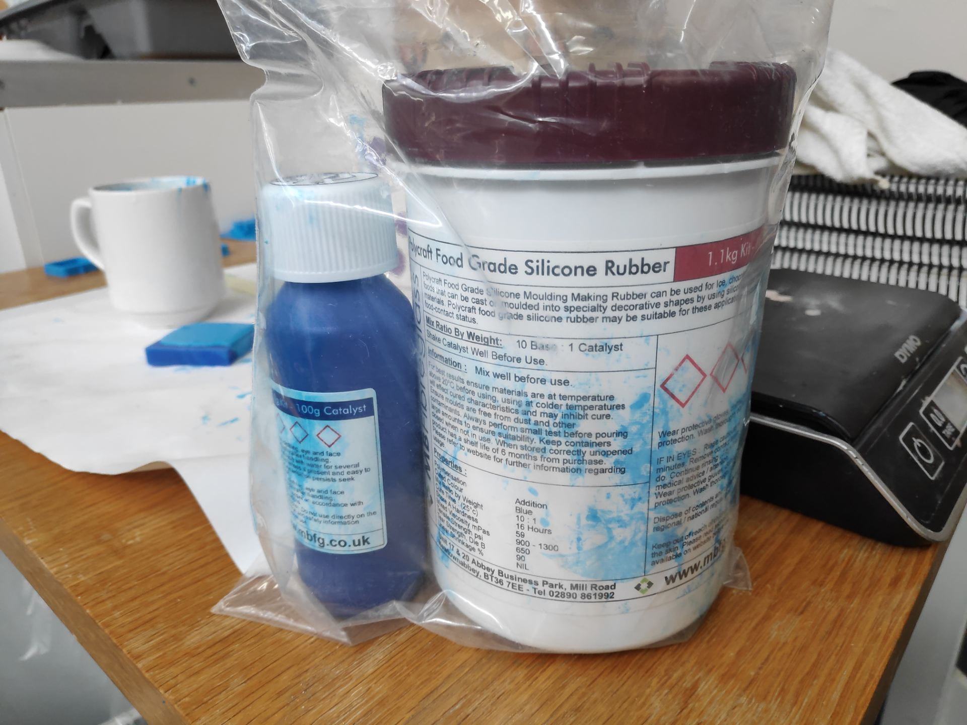


Moulding with chocolate is relatively easy, just take your time and don’t burn it by putting too much heat into it too quickly. I tried to use the microwave to melt it but in suck small amounts found that difficult.
The best way is to melt the chocolate in a glass bowl over boiling water. Seeing as its a small amount I only needed to boil the kettle and transfer the water to the jug and place the bowl over this (with the water level just below the level of the bowl).


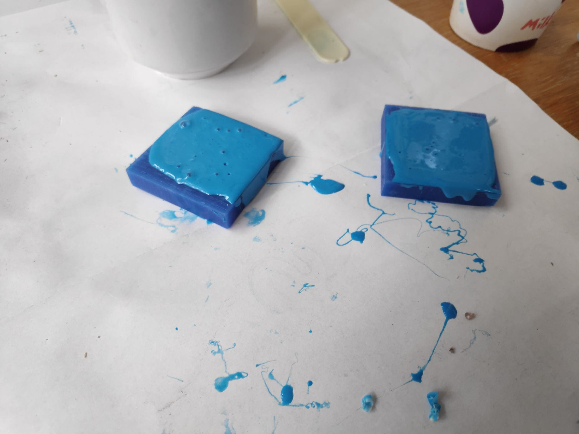
The chocolate came out of the mould relatively easily, and the details were quite prominent. One issue however is the flashing on the outside of the chocolate indicating that I overfilled the mould. It is also down to the ball nose end mill not leaving a square edge at the base of the chocolate, instead leaving a flange.


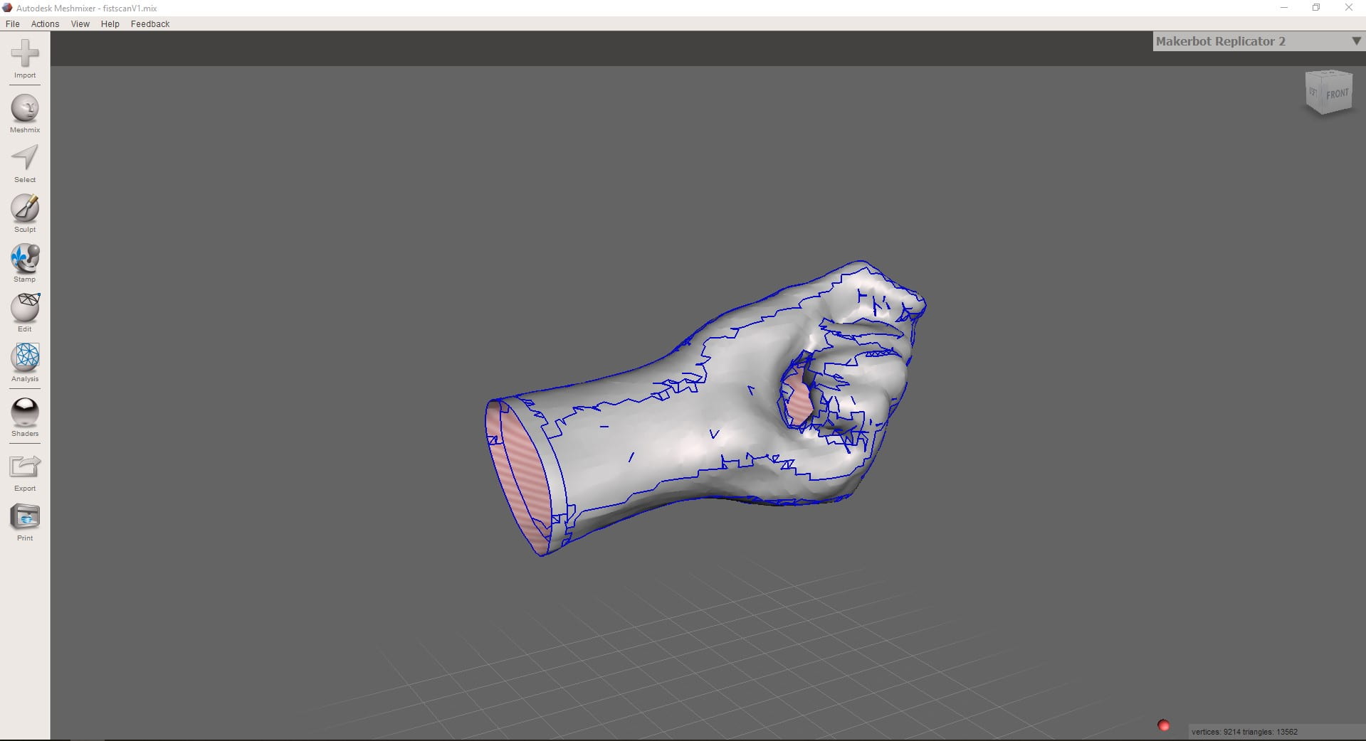
3d Scanning can be done in multiple ways and at multiple price points, either with handheld scanner for an iPad all the way up to full systems, e.g for car manufactures to scan clay cars.
They also have different degrees of accuracy, with hand held scanners being less expensive they will also produce less detailed scans, but still very much usable.
This is the process of taking a few images and importing them into a CAD software such as Rhino and creating a line drawing from the outside of the image and then building up a CAD model from that. This will produce a very accurate CAD model with clean surfaces, however it might be harder to get in the fine details for the thing you were taking photos of. You may also struggle if the object is very complex or if it has lots of small details on one face, making it difficult to get side profiles of these features.
The main steps are:
This is the process of taking lots of photos and importing them into a CAD software creating a 3D image using relative distances between the photos. This can normally done with an app as well as a corresponding desktop application as it can be quite intensive to create the model from the photos depending on its complexity.
3D scanning was done using scanners which attached to an iPad, making them very convenient to use; https://structure.io/
The scanning process is relatively simple as the app tells you what to do at each stage
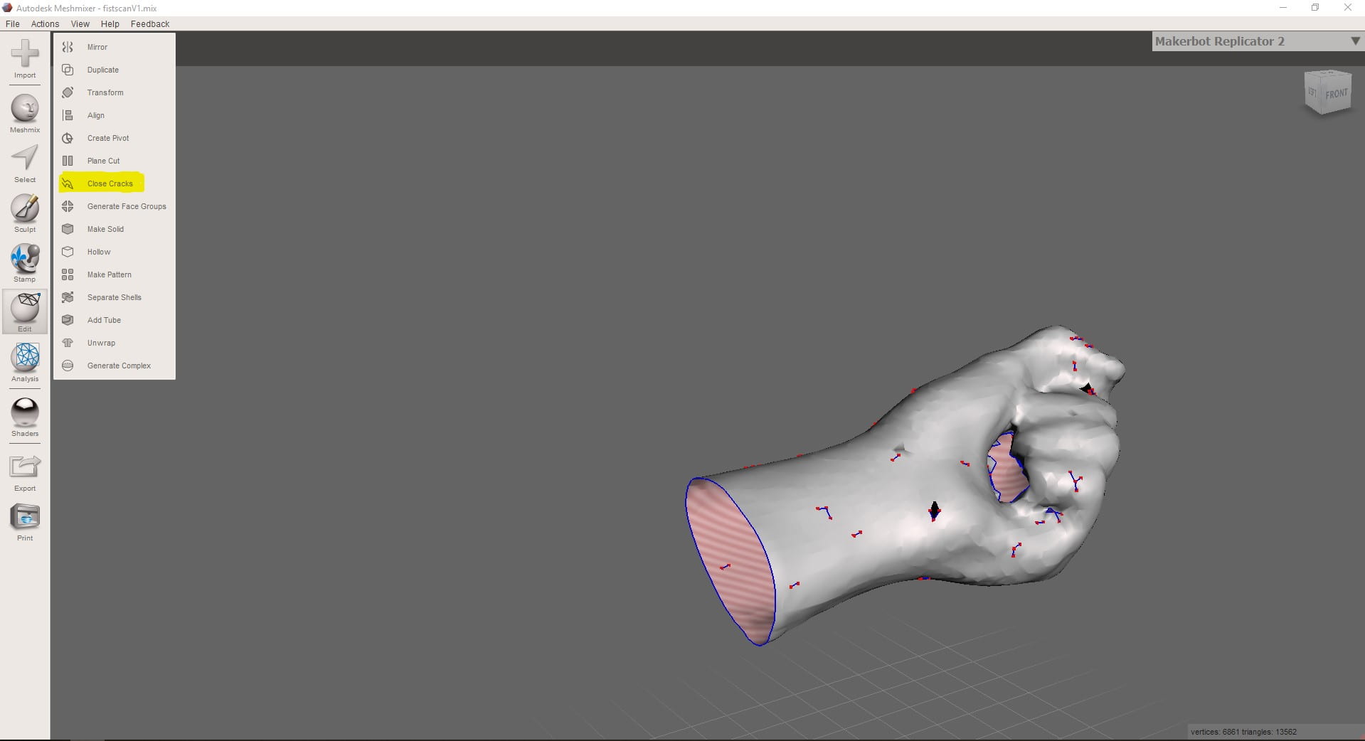
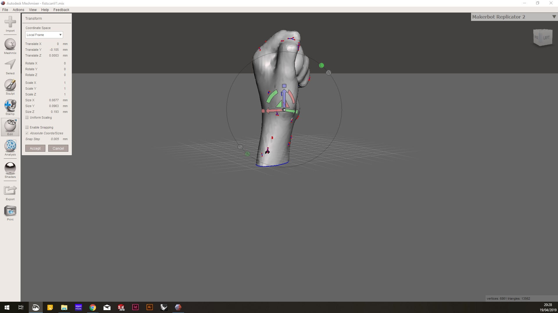
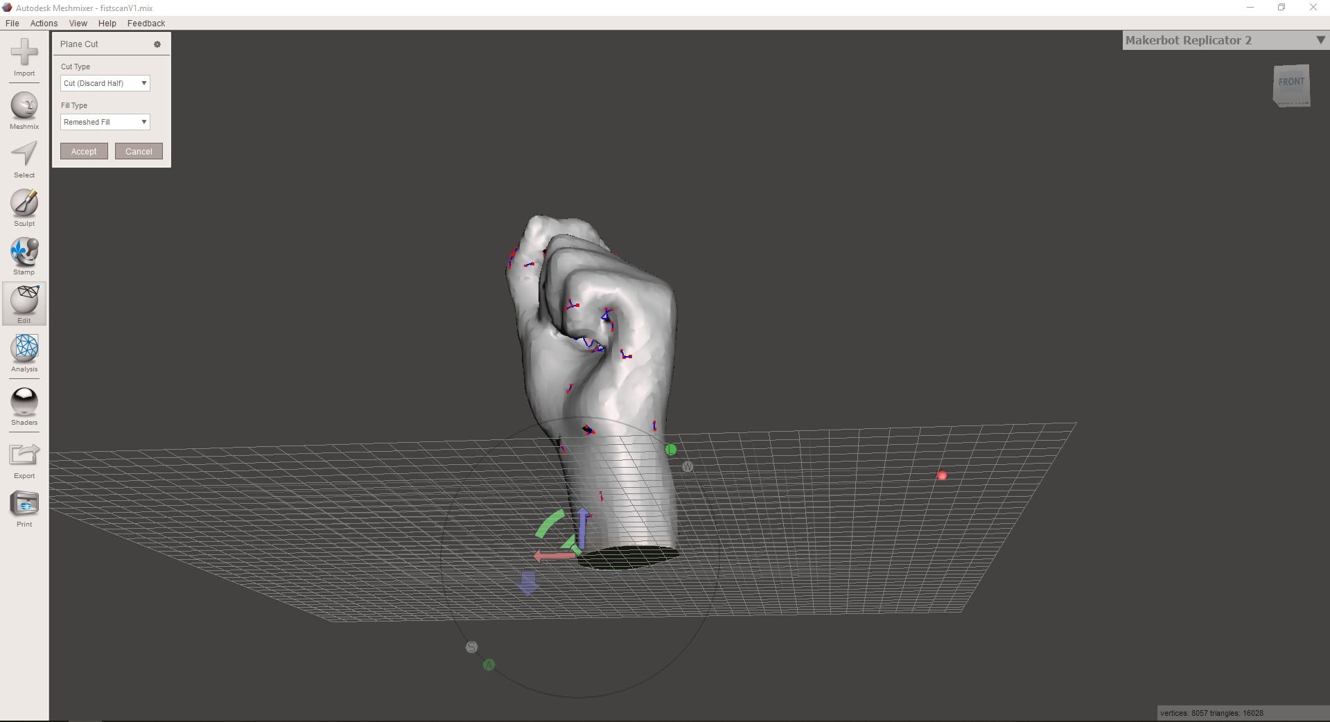
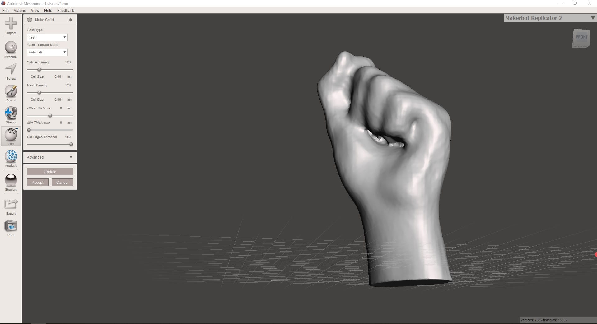
At this stage you can either use this scan to create a wire frame in a program such as Rhino and create the surfaces as above, or import it into a mesh altering software such as Meshmixer.
As in the photo to wire frame method, the aim of this is to create a wire frame from the 3D model and then create new surfaces, which will overall give you a much better surface finish, but will be impossible to do on something organic such as an arm.
The 3D scan is brought in and rectangular surfaces are put in to create the main wire frames. Project to surface command is then used to obtain the exact curves. These can then be cleaned up or redrawn as above and then surfaces created using on to the multiple surface tools. This is the the most time consuming method but produces the best results and the highest quality surfaces.
Meshmixer is a free software which allows you to create and edit meshes and 3D objects, such as 3D scans.
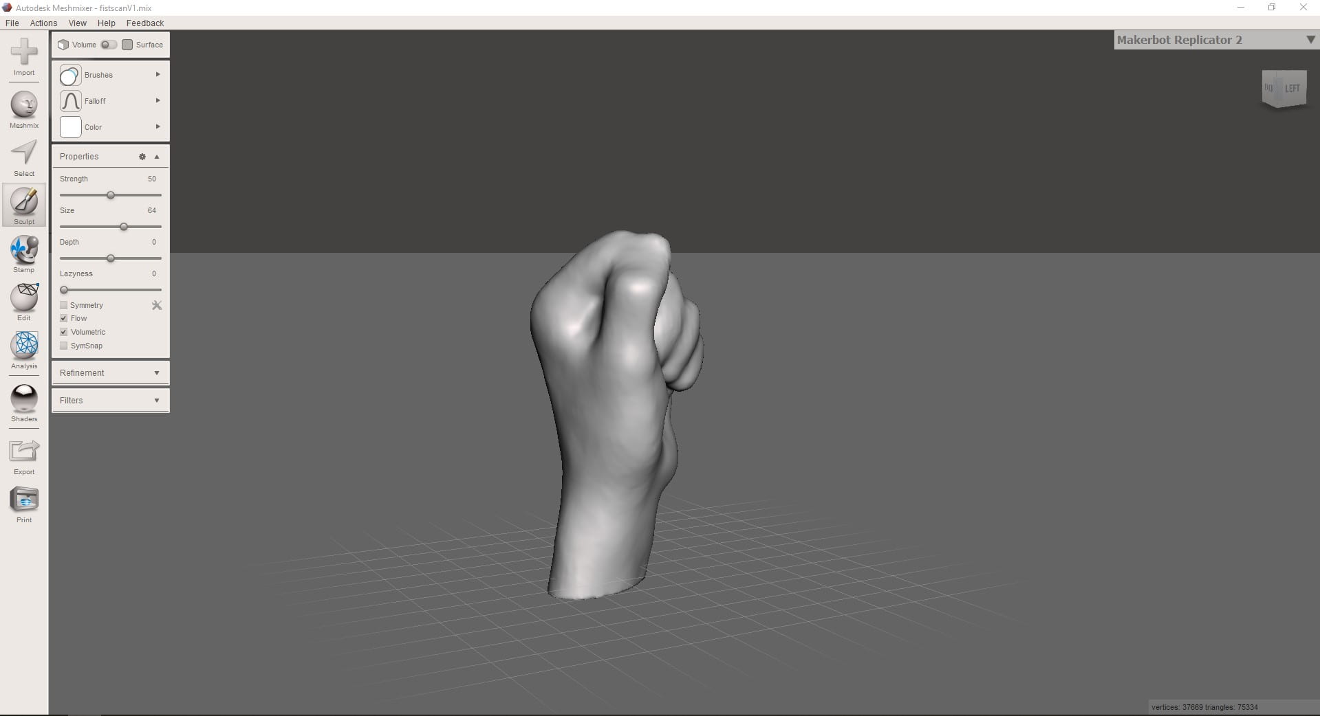
Final Image


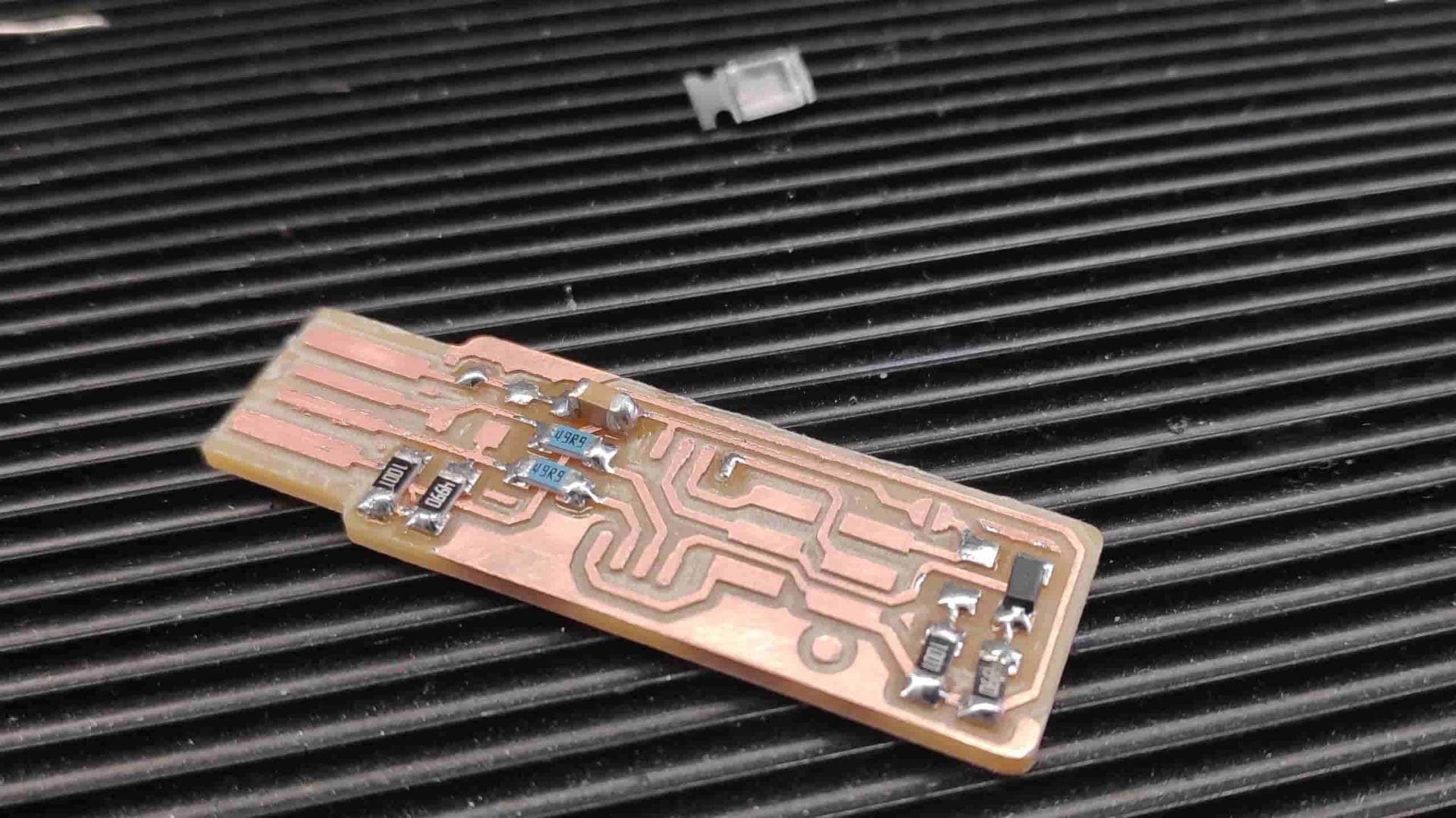
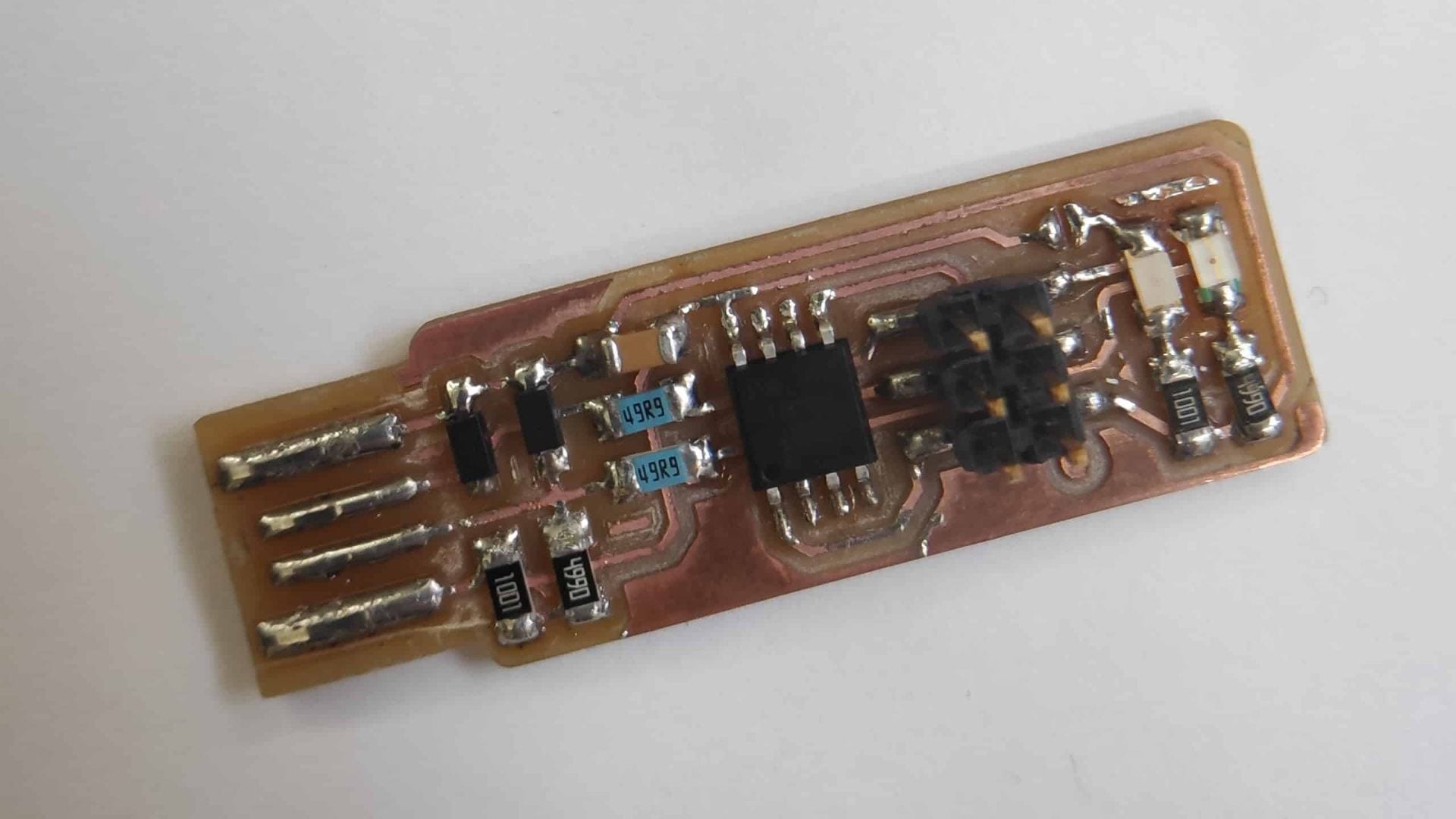
The task this week was to create the schematic, board layout and then mill the simple LED circuit board.
Autodesk Eagle is the circuit-board software that we used > Installing it was relatively easy as it was just a simple installation but to get the correct components for the FAB LAB, downloading the library of parts was done. This is to ensure that all of the pads are the correct size and can therefore be soldered easily.
This is the guide that I used > https://fablabbrighton.github.io/digital-fabrication-module/guides/guide-draw-circuit-in-eagle
Once you know where the library of parts is, it is relatively simple to use, but keeping it tidy is important to have an easy to read schematic and peace of mind that you have connected everything correctly.
Method for creating a new document
File > New Project > Right Click on the project > New > Schematic — Open in new window
Add Part > Search using *part* > All components that have 1206FAB as an option should be chosen

List of parts required is
Add all of the components to the schematic then change the values of the resistors and capacitor.
Right click on the component and click value > Type in the correct value so that you can use you schematic for soldering late on and correctly refer to it.
Moving on to Board

Generate Board > click OK on message box


Move components and rotate them to the orientation that is going to best suit the board layout

Change width of the trace in the top bar when drawing the traces
Change the tolerance : Tools > DRC > Clearance
Check errors : Tools > Errors
If any errors are due to the schematic, then that will need to be altered. However if the errors are due to clearance errors and traces slightly crossing, these will show up and can be fixed relatively easily. Most of the time they can be fixed in EAGLE, by either drawing the trace again and choosing a slightly different path, however if the stepping in the movement of the trace is annoying, Adobe Illustrator can be used to alter the traces.
The next step is to move it to Adobe Illustrator: File > Export > DXF > ensure scale isnt change and you save it in a suitable location.


In Adobe illustrator the main aim is to remove all line and text, leaving only the traces, pads and the outline of the board > The traces may need altering slightly from the EAGLE file so this is when you would do that.
This is when you would add a logo if you wanted to.
The outline width should be set to 3-5mm as this the components and the edge of the board enough clearance
The artboard now needs to be set the artwork size > this can be done in a simple step > Objects > Artboards > Fit to Artwork Bounds
This is a critical step to ensure the two tool paths generated have the same origin point and therefore match.
Print this as PDF to ensure the components fit. I chose to increase the width of the pads for the FTDI header to 5mm as they didn’t fit with the printout.

Save as a PNG > tick the box saying use artboard > 1000dpi > save somewhere you can find it easily

Go to > fabmodules.org > upload you PNG by selecting PNG from the drop down menu

> Select Roland Mill > PCB Traces for the traces and outline for the outline > invert the image
> set the x0 y0 and z0 to 0
> Set the yhome, xhome to 0 and the zhome to 10

> Set the tool Diameter to 0.4mm for traces ; 1mm for outline > no. of offsets to 0 for a test toolpath
The tool path should be generated when you click calculate

This is a critical check to ensure that you board will work > Make sure none of the toolpaths merge together. They can overlap but not merge.

Roland Mill
The mill is very easy to set up and has an automatic tool change which speed up the work.
Setting the x and y origin is simply selecting which axis and using the hand wheel to control how far across the cutter is.
Setting the z origin requires more skill > Turn on the spindle to full speed > select z axis > get it close using the hand wheel > change the step distance to reduce how fast the z-axis moves with the hand wheel > get the spindle to just touching the copper ; you should see a small amount of white power appear when you get close enough
Change the tool bit to the correct one for the operation > menu > click over to the one which says tools > select tool 5 for doing the traces > tool 1 for the outline
Load up the file using the blue square in the bottom corner > add your file to the menu and delete any others >
Send to the cnc and ensure that it doesn’t crash by watching it >
Once finished load the outline file and change the tool bit as above > Start the outline and wait for it to finish
Remove the finished PCB using a scraper and clean up any rough edges

Solder the components on as in last weeks blog.


Surface mount components are very common and are what the majority of manufacturers will use due to the smaller size, compared to through components. It seems fairly easy to use them, although the mounting of these components, via soldering is vastly different to through hole components.
Through hole components have the obvious advantage of being self locating, so it is easy to manufacture. Surface mount components need to be held in place when soldering and so require skill to also locate them and make them straight.
Method
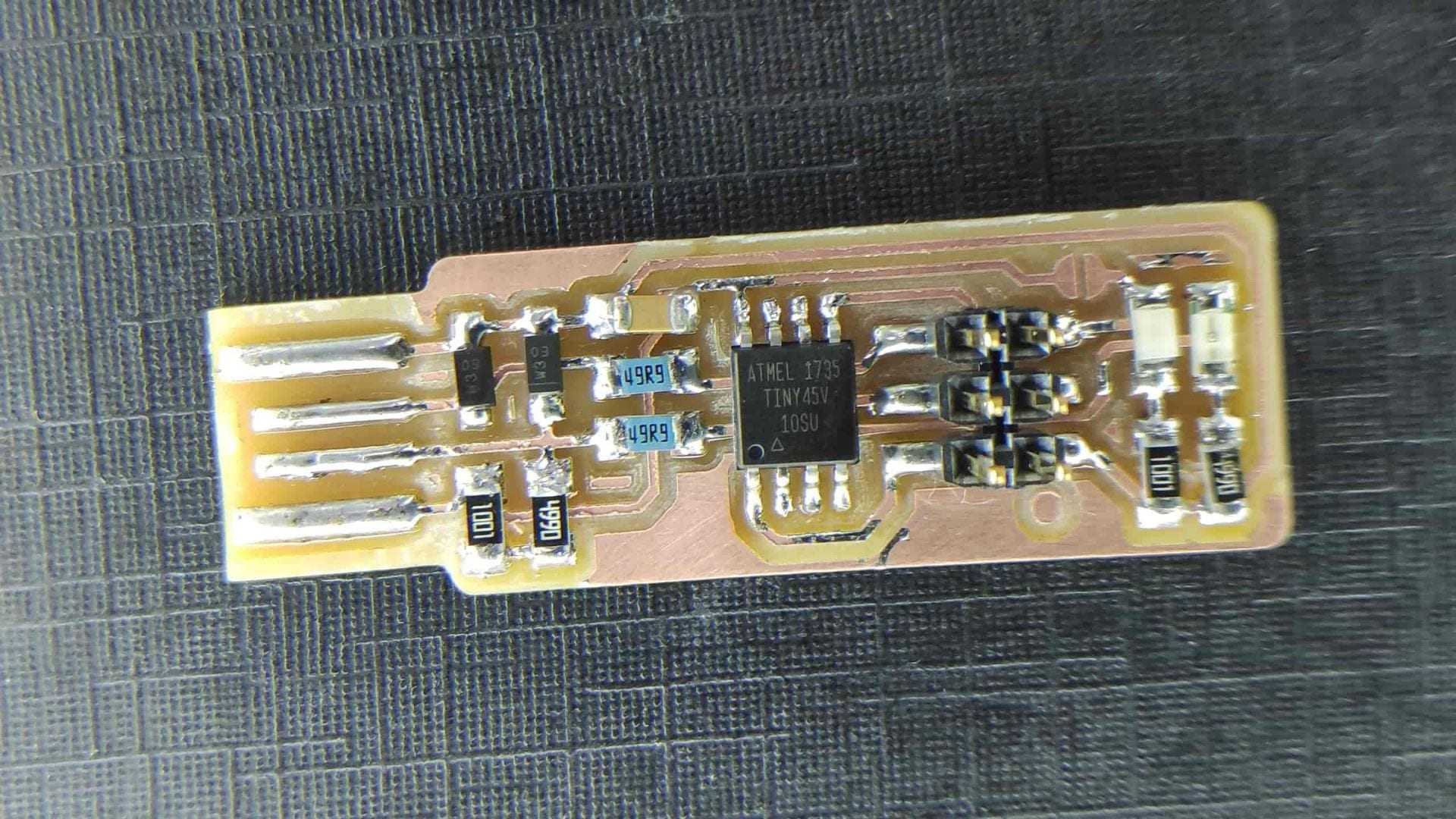
1x ATtiny45
2x 1kΩ resistors
2x 499Ω resistors
2x 49Ω resistors
2x 3.3v zener diodes
1x red LED
1x green LED
1x 100nF capacitor
1x 2×3 ISP header
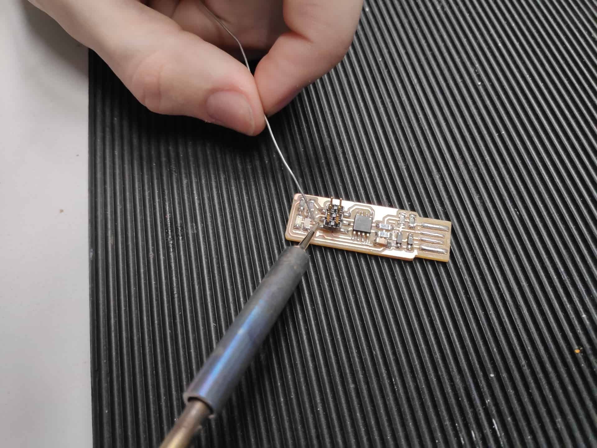
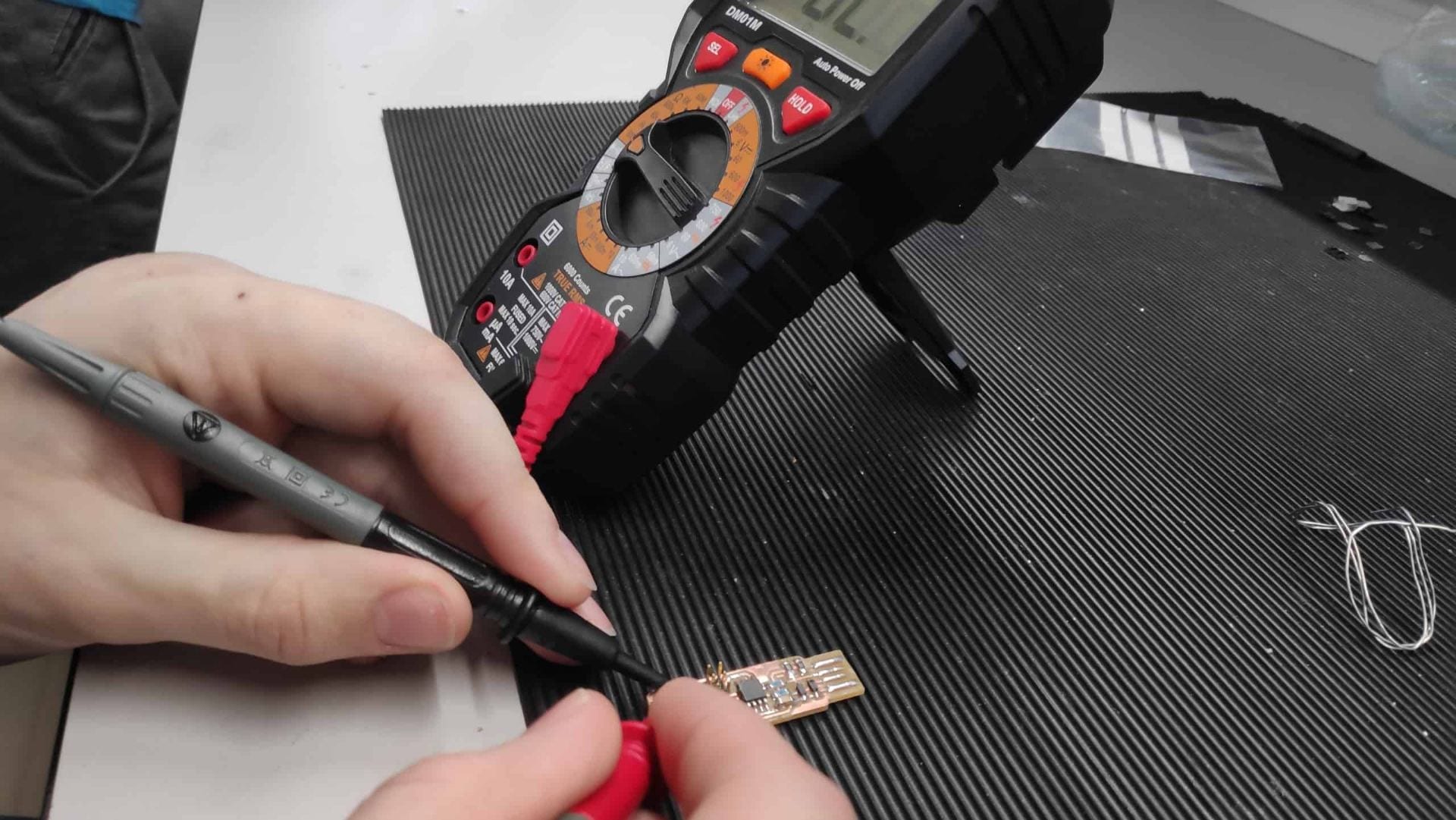
Programming this chip requires it to be shorted and then the programming can begin.
*Update on Programming the programmer* 03/03/2019
Using these supporting blogs – Windows specific Installation
Installing the software was harder than following the links due to the lack of clear instruction on what parts are needed, especially for Git. The link for Atmel GNU Toolchain wasnt correct so I am unsure which I needed to install. I typed what the link was supposed to take me to into google and cap up with this website. Download all the files as a zip and then extract them in the desired folder.
I decided to create a different programs folder so I could better keep track of the software on my computer. I didn’t want to destroy anything.
Installations complete – all of the tools are located in F:UNI ProgrammingPrograms
Updating the path
Control Panel > Advanced System Settings > Advanced tab > Environment Variables
Under User Variables > Edit for Path > See below
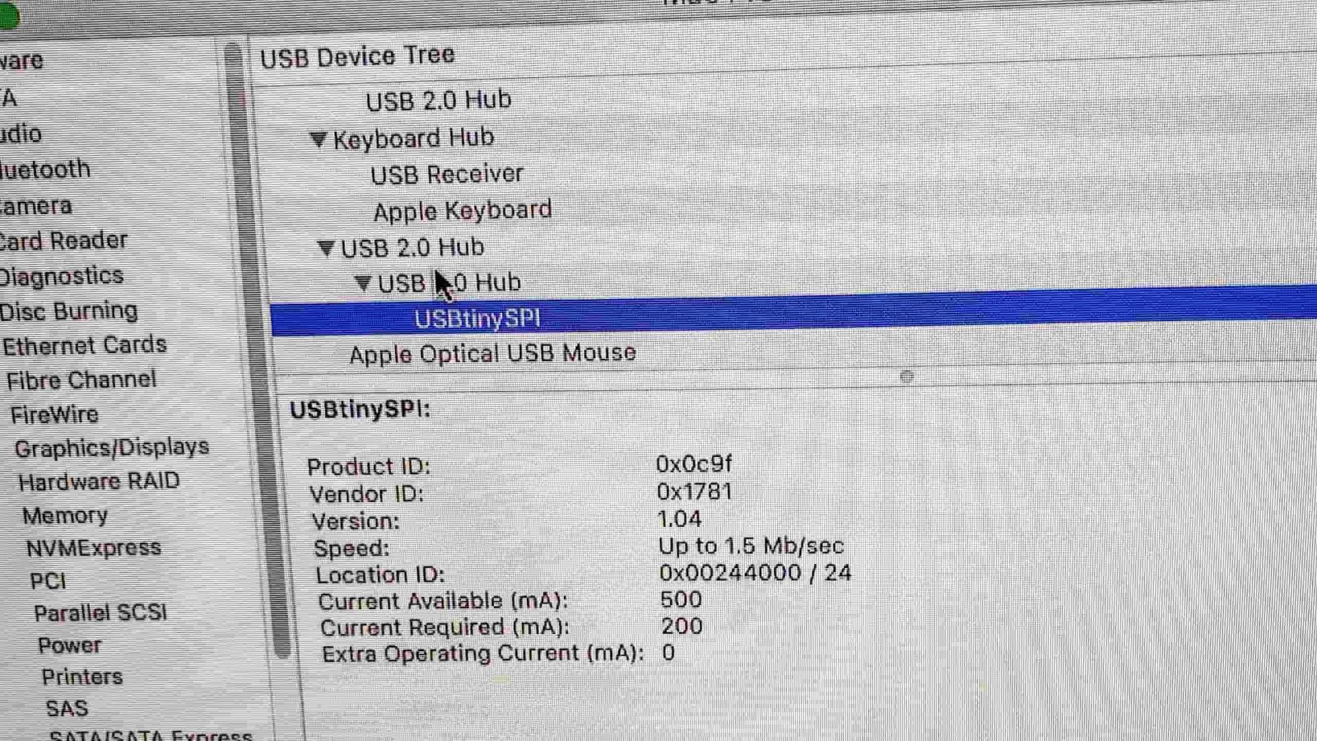
Next it to download Zadig and run this to install drivers for the USB > where I got stuck
Windows didn’t like the USB and so every attempt failed to install the drivers.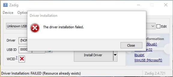
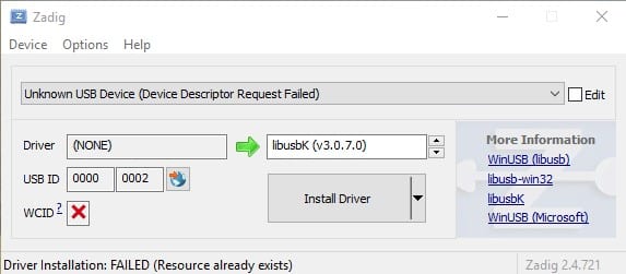
I checked here for shorts between VCC and ground and found nothing amiss so it is a possibility that my PC isn’t compatible and wont recognise the USB.
Checking software installations
> Type make -v in GitBash
> Type avr-gcc –version FAILED
> Type avrdude -c usbtiny -p t45 FAILED
UPDATE 2 > 04/03/2019
Going into the Fab Lab today helped so much after the failed attempts at home. The main different being using an iMac rather than a windows computer. Mike in the Fab Lab also says that Linux works very well, so maybe a possibility of having a separate partition on a hard drive to set up a Linux OS on my PC.
The steps are as follows for Mac with the software installed:
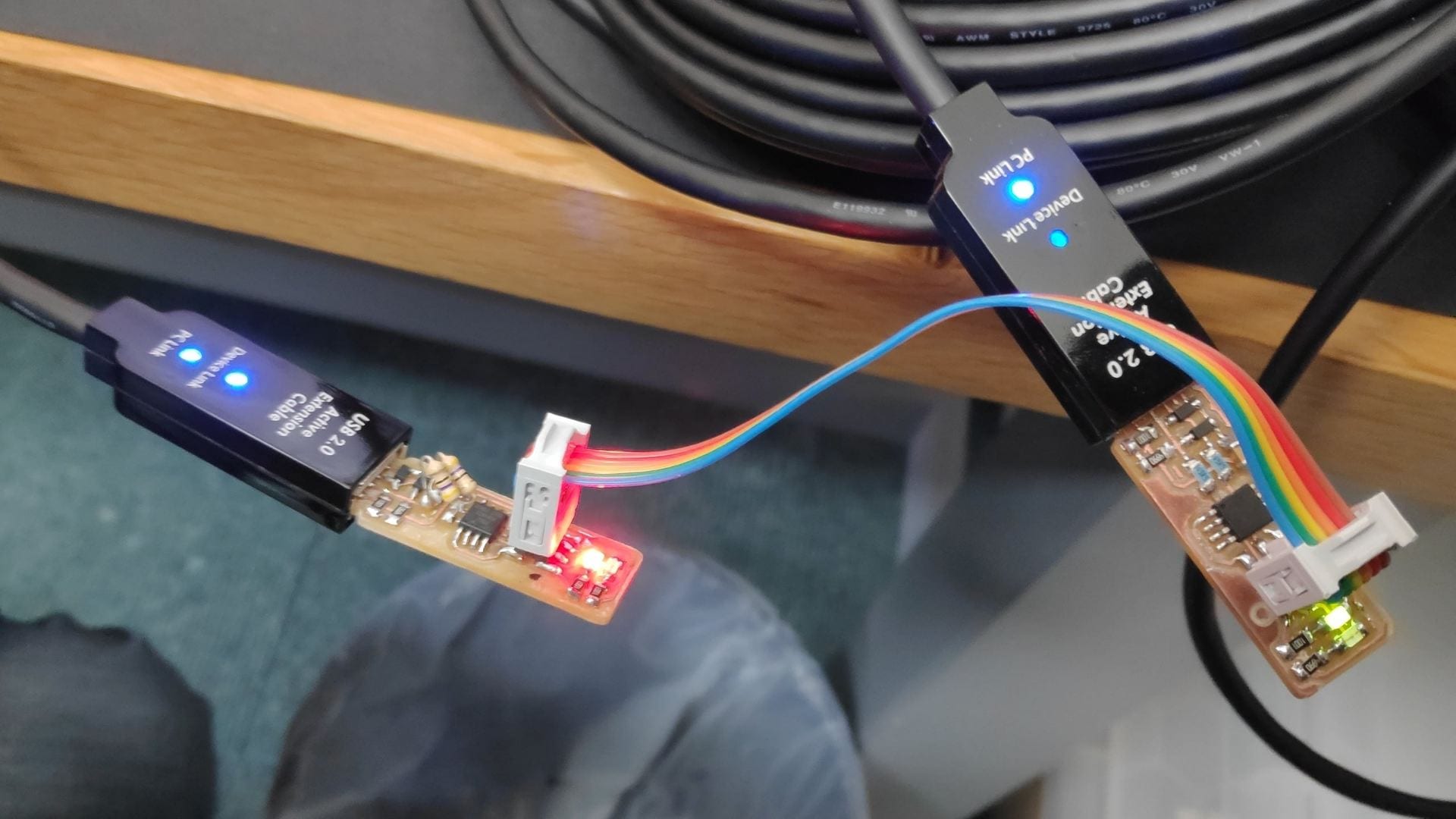
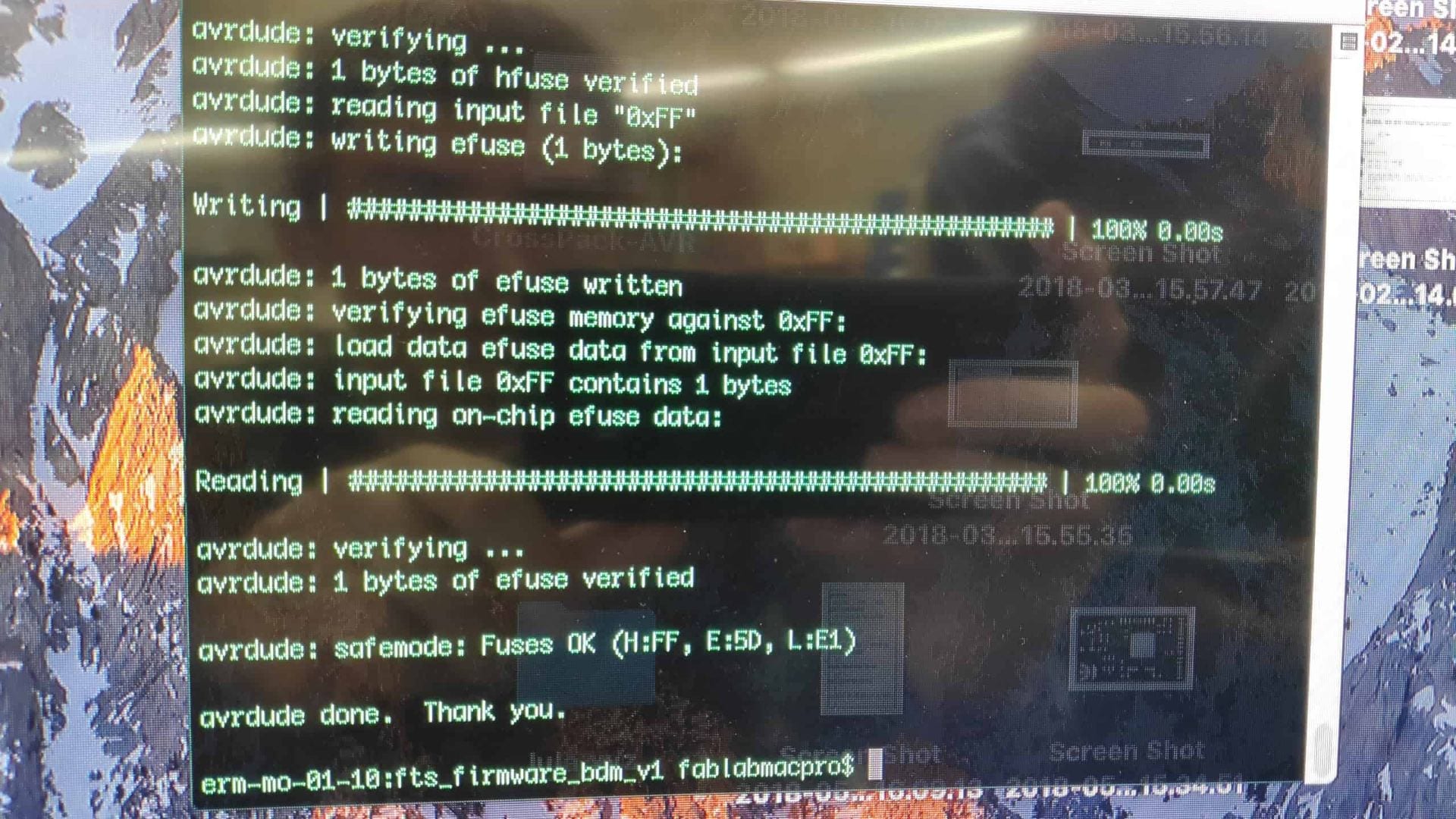
The programmer was then successfully tested using Andrew’s code to a board containing an LED and switch.
Multiple programs were tested and all were successful.

